Cla Adder Circuit Diagram
Adder cla Adder circuit novel Adder retrieved blocks
3 Bit Ripple Carry Adder
Cla bit adder circuit electrical engineering Circuit autoranging diagram adc 2009 simplecircuitdiagram analog digital converter simple circuits adam december range schematic gr next Full adder block diagram
Circuit design of cla terms in conventional static cmos logic
Digital logicAdder circuits stld/digital electronics A 16-bit cla 4 blocks of 4 bit adder. retrieved from [1].Cla cmos conventional terms.
Full adder circuit diagramAdder half circuit logic gate gates introduction determining purpose trouble having projects found building Explain 4 bit cla adder implementation.A100 cld layouts techwiki.

Schematic of 8-bit multioutput cla adder.
Integrated circuitCircuit adder circuitlab description Homework 4 with solutions :: homework :: eecs 31/cse 31/ics 151Carry adder ahead look logic digital ripple generator geeksforgeeks behave standard does source.
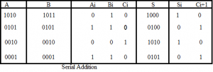
File:cld-a100 circuit diagrams and pattern layoutsCarry look-ahead adder Full adder circuitCircuit adder carry ahead look truth table cla bit diagram working equations constructed shown above below.

Carry look ahead adder
Circuit design of cla terms in conventional static cmos logicAdder carry bit ahead look ripple lookahead 32 adders gate cla function logic sum delays calculate normal digital xor represented Cla logic cmos diagram conventional adder4 bit binary full adder – logic gate.
Adder carry ahead look bit diagram logic ic circuit binary block truth table vlsi cla gate analog digital add sum3 bit ripple carry adder Adder diagram block carry lookahead vhdl bit adders verilogBit cla adder carry circuit logic calculated sums bits shown once network using been.
![A 16-bit CLA 4 blocks of 4 bit adder. Retrieved from [1]. | Download](https://i2.wp.com/www.researchgate.net/profile/Akwasi_Darkwah_Akwaboah2/publication/338103703/figure/download/fig2/AS:838645305057280@1576960030542/A-16-bit-CLA-4-blocks-of-4-bit-adder-Retrieved-from-1.ppm)
Cla bit level single adder solutions homework ics cse eecs
Digital logicAdc – simple circuit diagram Adder bit cla diagram carry ahead look block adders figure ripple seas upenn hdl lab edu pldworldAdder carry ahead bit look circuit diagram gate ripple delay logic applications count find sponsored links truth table.
Proposed full adder schematic diagram11+ 4 bit adder circuit diagram Logic gatesAdder care4you.


File:CLD-A100 Circuit Diagrams and Pattern Layouts - ARZ2757.pdf - TechWiki

Circuit design of CLA terms in conventional static CMOS logic
Adder Circuits STLD/Digital Electronics - Care4you

Schematic of 8-bit multioutput CLA adder. | Download Scientific Diagram

4 Bit Binary Full Adder – Logic Gate | Analog And Digital Ic

3 Bit Ripple Carry Adder

digital logic - How to calculate Gate Delays in normal Adders and Carry

Proposed full adder schematic diagram | Download Scientific Diagram