Circuit Diagram Of Ram Memory
Ram logic memory diagram powerpoint programmable ppt presentation fig Memory ram access random circuit emulator following address vhdl code addresses holding Ram cpu bit chips basic benningtons using bits each two
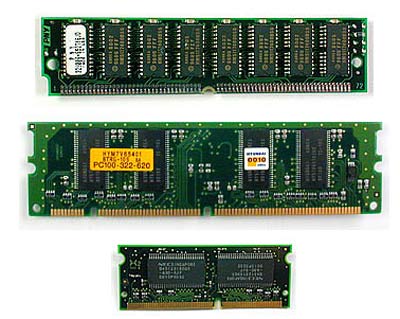
Memory | electro,circuit, schema & Datasheet
Ram diagram memory slot parts computer pc hardware function components cpu 9i 2010 contacts troubleshooting gold february Virtual lab for computer organisation and architecture Memory address decoding
Ram memory random access circuit study supplier india exporter manufacturer
Memory schematicInternal implementation multisim Random memory access (ram) emulator: the followingRam diagram circuit section its motherboard solution problem desktop 2525 2526 diagnostic card show.
8-bit cpu – ram « benningtons.net64k solved Ram memory cell binary watson write read circuits input random access bc line output figure select latech eduRam memory access random structure memories.

Bablu patel: ram section circuit diagram and its problem solution in
Bablu patel: ram section circuit diagram and its problem solution inUsing chips ram 16 32 construct schematic circuit logic digital address x4 electronics parallel lines circuitlab created S100 computersMemory 8085 microprocessor mapping interfacing system.
Memory ram chip main diagram block typical chips javatpoint coa per capacityRam diagram section circuit motherboard desktop its ddr solution problem 2v Circuit translation: 16 by 4 bit memoryMemory circuit bit schematic 16 diagram entryway applications.

Explain ddr3
Ram block diagram1 bit memory cell in 555 timer ic Memory circuit computer circuits gr next frame processing digital cooperate signal temporarily needs work whenMemory circuit electro datasheet schema storage.
Ram memory structure random access basic write ppt read powerpoint presentation chip logic data register lines address select(pdf) implementation of storage device (ram) using multisim Decoding eprom execution jmp occurs startsMemory schematic schematics.

Digital logic
Memory write read ram vlsi circuit memoriesDimm ram ddr3 memory test random access module sodimm tester computer modules eli5 why need testing ddr2 adapter object physical Ram (random access memory) structureRam block diagram.
Study of ram random access memory circuit manufacturer, supplierMemory circuit : computer circuits :: next.gr Memory circuit bit cell diagram ic using timerMemory ram and slot diagram.

32k 8086 8088 interface decoding
Extending the ram memory of a pic microcontroller « dangerous prototypesMemory mapping Ram memory extending pic microcontroller circuit circuits sram gr next repositoryRam circuit fpga v2.
Memory ram circuit diagram computer 4x3 architecture virtual lab iitkgpMemory ram does work random access sdram refresh dram cells stack Eli5: why do we need ram, what is *random* access memory, and what isMemory address decoding.


(PDF) IMPLEMENTATION OF STORAGE DEVICE (RAM) USING MULTISIM

Bablu Patel: RAM Section Circuit Diagram and Its Problem Solution in

Memory Schematic

memory circuit : Computer Circuits :: Next.gr
Memory | electro,circuit, schema & Datasheet

Memory Address Decoding

PPT - Random-Access Memory (RAM) PowerPoint Presentation, free download